
Table of Contents >> Show >> Hide
- Introduction: Why TTL Still Sneaks Into FPGA Conversations
- What TTL Means in Digital Electronics
- TTL Voltage Levels: The Heart of the Matter
- TTL Noise Margin: Breathing Room for Real Signals
- Input Current, Output Current, and Fan-Out
- Propagation Delay: TTL Is Fast, But Not Magical
- TTL, LVTTL, CMOS, and HCT: The Alphabet Soup
- Connecting TTL Signals to FPGA Inputs
- Connecting FPGA Outputs to TTL Inputs
- Open-Collector TTL and Pull-Up Resistors
- Schmitt Trigger Inputs: Cleaning Up Slow or Noisy TTL Signals
- Power Supply and Decoupling for TTL Systems
- Signal Integrity: When Digital Stops Looking Digital
- Practical Example: Reading a 5 V TTL Sensor With a 3.3 V FPGA
- Practical Example: Driving an Old TTL Board From an FPGA
- Common Mistakes When Moving From Gates to FPGAs
- Design Checklist for TTL-to-FPGA Interfaces
- Experience Notes: Lessons From Real TTL-to-FPGA Work
- Conclusion: TTL Knowledge Still Belongs in the FPGA Toolbox
Note: This article synthesizes real engineering concepts from manufacturer datasheets, FPGA I/O user guides, and logic-family application notes into original, publication-ready educational content.
Introduction: Why TTL Still Sneaks Into FPGA Conversations
TTL logic is the electronics equivalent of that old pickup truck in the neighborhood: not new, not flashy, but somehow still showing up at important jobs. Even in a world full of low-voltage FPGAs, high-speed serial links, DDR memory, and tiny chips that look like black sesame seeds with legs, Transistor-Transistor LogicTTLstill matters. Why? Because many designers eventually need to connect modern programmable logic to older boards, lab equipment, industrial controllers, vintage computing hardware, microcontroller modules, or 5 V digital signals that refuse to retire gracefully.
The phrase “Gates To FPGAs: TTL Electrical Properties” sounds like a bridge between two eras. On one side, you have classic 7400-series logic gates: NANDs, NORs, inverters, flip-flops, counters, and bus drivers. On the other, you have FPGAs: configurable oceans of logic blocks, routing fabric, I/O banks, and timing constraints. The trouble is that digital logic is not only about ones and zeros. It is also about volts, amps, thresholds, timing, drive strength, noise margin, and whether a poor little input pin is about to receive more voltage than it signed up for.
This article explains TTL electrical properties in a practical way, especially for engineers, students, makers, and hardware designers moving from simple gates to FPGA-based systems. We will look at voltage levels, input and output currents, fan-out, propagation delay, noise margins, interfacing rules, and the big question that keeps many FPGA pins awake at night: “Can I connect this 5 V TTL signal directly?” Spoiler alert: sometimes the answer is “maybe,” but the professional answer is usually “read the datasheet before the magic smoke files a resignation letter.”
What TTL Means in Digital Electronics
TTL stands for Transistor-Transistor Logic, a family of digital logic circuits historically built using bipolar junction transistors. Classic TTL became famous through the 7400 series, which included simple gates and more complex building blocks. The original TTL family was followed by improved versions such as Low-Power Schottky TTL, commonly known as 74LS, and Advanced Low-Power Schottky, often called 74ALS.
At the circuit level, TTL inputs and outputs behave differently from CMOS logic. TTL inputs draw current in ways that can surprise designers who are used to near-zero CMOS input current. TTL outputs also have asymmetric drive capability: they usually sink current better than they source it. In plain English, a TTL output is often stronger when pulling a signal low than when pushing it high.
That matters when you connect TTL gates to FPGAs. Modern FPGAs are built mainly with CMOS technology and commonly operate their I/O banks at 3.3 V, 2.5 V, 1.8 V, or lower. Some older or special-purpose FPGA boards may tolerate certain 5 V signals, but many do not. This is where TTL electrical properties become less like trivia and more like “please do not destroy the board before lunch.”
TTL Voltage Levels: The Heart of the Matter
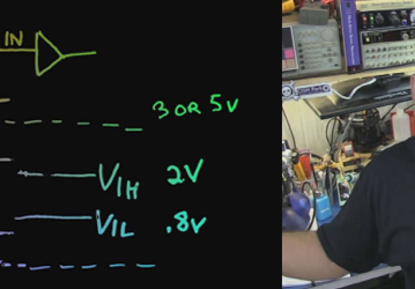
The most important TTL electrical properties are the logic voltage thresholds. Digital circuits call signals “high” or “low,” but the real world sends voltage ranges, not polite little labels.
Standard TTL Input Levels
For classic 5 V TTL logic, a low input is generally recognized when the input voltage is at or below approximately 0.8 V. A high input is generally recognized when the voltage is at or above approximately 2.0 V. The region between those values is undefined. It is not a secret third logic state called “emotional support voltage.” It is simply a danger zone where the device may behave unpredictably.
This is one reason TTL is relatively friendly to 3.3 V logic in one direction. A 3.3 V CMOS output can usually drive a TTL input high because TTL only needs about 2.0 V to recognize a high. However, the reverse direction is not always safe. A 5 V TTL output connected to a 3.3 V FPGA input may exceed the FPGA pin’s absolute maximum rating unless the pin is designed to tolerate it or the circuit includes protection.
Standard TTL Output Levels
TTL output voltage levels are also specified as ranges. A TTL output low is typically close to ground and is usually guaranteed below about 0.4 V under rated load. A TTL output high may be guaranteed above about 2.4 V, not necessarily all the way to 5 V. That surprises many beginners. A TTL “high” does not have to mean 5 V; it only has to be high enough for another TTL input to understand.
This detail becomes important when a TTL output drives CMOS logic. Standard CMOS inputs powered at 5 V may require a much higher voltage to recognize a logic high, often around 70% of the supply voltage depending on the family. That means a TTL output high of 2.4 V may not reliably drive a 5 V CMOS input. This mismatch is one reason HCT logic exists. HCT devices are CMOS internally but use TTL-compatible input thresholds, making them useful translators between older TTL-style signals and CMOS systems.
TTL Noise Margin: Breathing Room for Real Signals
Noise margin tells you how much unwanted voltage disturbance a digital signal can tolerate before logic errors become likely. It is the difference between what one device guarantees at its output and what the next device requires at its input.
For a TTL high signal, the output may be guaranteed to reach at least about 2.4 V, while the receiving TTL input requires at least about 2.0 V. That gives roughly 0.4 V of high-level noise margin. For a TTL low signal, the output may be guaranteed at or below about 0.4 V, while the receiving input accepts up to about 0.8 V as low. That also gives roughly 0.4 V of low-level noise margin.
In a clean lab circuit with short wires, 0.4 V can be plenty. In a noisy industrial cabinet with long cable runs, motors, relays, and grounding that looks like it was designed during a thunderstorm, 0.4 V starts looking less luxurious. This is why good PCB layout, proper grounding, decoupling capacitors, controlled edge rates, and clean power rails matter.
Input Current, Output Current, and Fan-Out
TTL is not only about voltage. Current matters too. Classic TTL inputs require current, especially when pulled low. A TTL output must supply or sink enough current to drive all connected inputs while maintaining valid logic levels.
What Fan-Out Means
Fan-out is the number of inputs that one output can reliably drive. In classic TTL systems, fan-out was often calculated using input and output current ratings. If one TTL input requires a certain amount of current and one TTL output can sink or source a limited amount, you divide the output capability by the input requirement to estimate how many gates can be connected.
Modern CMOS inputs draw very little steady-state current, so fan-out is often limited more by capacitance, signal speed, and edge quality than by DC current. But when working with real TTL, especially older parts, input current remains a real design number. Ignore it and the circuit may still workuntil temperature changes, the power supply droops, or the universe decides your prototype needs character development.
TTL Outputs Sink Better Than They Source
Many TTL outputs can sink significantly more current than they can source. This is why old TTL designs often used pull-up arrangements, active-low signaling, and LED connections where the TTL output pulled current down through the LED. If you have ever seen logic signals with bars over their names, such as /RESET or /CS, you have met the active-low lifestyle.
When connecting TTL outputs to FPGA inputs, the FPGA input current is usually tiny, so DC loading is rarely the main problem. Voltage tolerance is the bigger issue. When connecting FPGA outputs to TTL inputs, the key question is whether the FPGA output voltage is high enough and whether it can meet the input current requirements of the TTL device.
Propagation Delay: TTL Is Fast, But Not Magical
TTL gates do not switch instantly. Every logic gate has propagation delay, the time between a change at the input and the resulting change at the output. In 74LS logic, propagation delays commonly fall in the nanosecond range, depending on the specific part, load, temperature, and supply voltage.
When designs grow from simple gates into counters, state machines, or bus interfaces, those delays add up. A signal may pass through several gates before reaching a flip-flop. If the timing is too tight, the flip-flop may sample the wrong value. This is where FPGA designers have an advantage: FPGA tools perform static timing analysis and can report whether paths meet timing. But when an FPGA interfaces with external TTL hardware, the external delays still matter.
For example, suppose an FPGA sends an address to a board full of TTL logic, then samples a returned data signal. The designer must account for FPGA output delay, PCB trace delay, TTL gate delay, possible bus driver delay, and FPGA input setup time. The logic may look simple on a block diagram, but electricity does not read block diagrams. It reads physics.
TTL, LVTTL, CMOS, and HCT: The Alphabet Soup
The transition from gates to FPGAs introduces several logic families and standards that sound similar but are not interchangeable.
TTL
Traditional TTL usually refers to 5 V bipolar logic such as 7400 or 74LS families. It uses TTL voltage thresholds and has input/output current characteristics associated with bipolar transistor logic.
LVTTL
LVTTL means Low-Voltage TTL. It is commonly associated with 3.3 V I/O systems and TTL-like switching thresholds. Many FPGA I/O banks support LVTTL as a selectable I/O standard. LVTTL is not the same as connecting any old 5 V TTL signal directly. The “LV” part is doing serious work in that name.
LVCMOS
LVCMOS is Low-Voltage CMOS. It is widely used in FPGA I/O standards at 3.3 V, 2.5 V, 1.8 V, and lower. LVCMOS inputs generally use CMOS-style thresholds related to the I/O bank voltage, although exact values depend on the FPGA family and selected standard.
HCT
HCT devices are high-speed CMOS logic with TTL-compatible input thresholds. They are extremely useful when a TTL output needs to drive CMOS-style logic without threshold drama. Think of HCT as the bilingual friend who speaks both “old 5 V board” and “modern CMOS conversation.”
Connecting TTL Signals to FPGA Inputs
The most common practical question is simple: can a TTL output drive an FPGA input? The answer depends on the FPGA’s I/O bank voltage, absolute maximum ratings, input standard, and whether the pin is 5 V tolerant.
Many modern FPGAs are not 5 V tolerant. A classic TTL output may produce a high level that rises near 5 V when lightly loaded. If that signal is connected directly to a 3.3 V FPGA input, current may flow through protection diodes or internal structures. Sometimes the board seems to work on the bench, which is electronics’ most mischievous way of saying, “I have not failed yet.” Long-term reliability can still be compromised.
Safer methods include using a resistor divider, a dedicated level shifter, a 5 V tolerant buffer, an HCT/LVC family interface device, or an FPGA input configuration specifically documented to handle the signal. For slower signals, a simple resistor divider may be acceptable. For faster edges, bidirectional buses, or timing-sensitive interfaces, a proper translator or buffer is usually the better engineering choice.
Connecting FPGA Outputs to TTL Inputs
Driving TTL inputs from an FPGA output is often easier. If the FPGA I/O bank is powered at 3.3 V and configured as LVTTL or compatible LVCMOS, its high output level is typically well above the TTL input-high requirement of about 2.0 V. The low output level should also be comfortably below the TTL low threshold.
However, current still matters. A single FPGA pin may drive one or a few TTL inputs without trouble, but loading many TTL inputs can exceed recommended output current or distort edges. If several TTL loads must be driven, use a buffer. Good hardware design is not about proving a pin can survive an unreasonable situation once; it is about making the circuit reliable on a hot day, with a marginal cable, after the customer has already printed the invoice.
Open-Collector TTL and Pull-Up Resistors
Some TTL outputs are open-collector. Instead of actively driving both high and low, an open-collector output can pull the line low but needs an external pull-up resistor to create a high level. This allows multiple outputs to share a line in wired-AND configurations, commonly used for interrupts, ready signals, and bus arbitration.
When connecting open-collector TTL to an FPGA, the pull-up voltage must be chosen carefully. If the pull-up goes to 5 V and the FPGA input is not 5 V tolerant, that is a problem. A pull-up to 3.3 V may work if all connected devices recognize 3.3 V as high. The resistor value must also be selected to balance current, rise time, and noise immunity. Too weak a pull-up creates slow edges; too strong a pull-up wastes current and may exceed what the open-collector device can safely sink.
Schmitt Trigger Inputs: Cleaning Up Slow or Noisy TTL Signals
A Schmitt trigger input adds hysteresis, meaning it uses different thresholds for rising and falling transitions. This is helpful when signals are slow, noisy, or generated by switches, sensors, long wires, or human beings pressing buttons with all the electrical elegance of a tiny earthquake.
If a TTL-like signal has a slow edge, feeding it into a normal FPGA input can cause multiple transitions or extra switching current near the threshold. A Schmitt trigger buffer can clean up the edge before it reaches the FPGA. Some FPGA families offer input hysteresis options for certain I/O standards, but availability depends on the device. When in doubt, use an external Schmitt trigger buffer and let the FPGA enjoy a cleaner digital life.
Power Supply and Decoupling for TTL Systems
TTL logic is usually associated with a 5 V supply. Classic TTL parts often expect a supply around 5 V with a relatively narrow tolerance. Modern FPGA I/O banks may use several different voltages, and each bank must be powered according to the chosen I/O standard.
Decoupling capacitors are essential. TTL gates can draw sharp current spikes when switching. Place small ceramic capacitors close to the power pins of logic ICs, and use proper power distribution on the board. A common beginner mistake is assuming a schematic wire labeled “5V” has zero impedance. It does not. PCB traces, vias, connectors, and breadboard contacts all add resistance and inductance. The faster the edge, the more those tiny imperfections act like unpaid interns creating problems nobody asked for.
Signal Integrity: When Digital Stops Looking Digital
At low speeds and short distances, TTL signals can be forgiving. At higher speeds or longer trace lengths, signal integrity becomes important. Fast edges can cause ringing, overshoot, undershoot, crosstalk, and ground bounce. These effects can violate input limits or create false switching.
FPGAs often allow designers to choose output drive strength and slew rate. A slower slew rate can reduce ringing and electromagnetic interference, while a faster slew rate may be needed for timing. The best choice depends on trace length, load capacitance, connector type, termination, and timing margin. The phrase “set everything to maximum drive” is not a design strategy. It is a way to turn a board into a radio station with delusions of grandeur.
Practical Example: Reading a 5 V TTL Sensor With a 3.3 V FPGA
Imagine a sensor board outputs a 5 V TTL-compatible pulse signal. The FPGA board uses 3.3 V I/O and does not clearly state that its pins are 5 V tolerant. The TTL high threshold is easy for the FPGA to detect, but the voltage may be unsafe. A simple solution for a low-frequency signal is a resistor divider, such as a top resistor from the sensor output to the FPGA input and a bottom resistor from the FPGA input to ground. The divider scales 5 V down to about 3.3 V or less.
For a faster signal, the divider’s resistance and input capacitance may slow the edge. A better option could be a 5 V tolerant logic buffer or dedicated level translator. If the signal is open-collector, pull it up to 3.3 V instead of 5 V, provided the sensor output transistor can operate correctly and the sensor’s documentation allows it.
Practical Example: Driving an Old TTL Board From an FPGA
Now imagine an FPGA must control an old 74LS-based peripheral board. The FPGA outputs 3.3 V logic. Since classic TTL inputs usually recognize anything above about 2.0 V as high, 3.3 V is generally enough. The FPGA low level should also be accepted as a valid TTL low.
The main concern is loading. If one FPGA output drives many TTL inputs, check the TTL input current and the FPGA output drive rating. If the load is too heavy, add a buffer such as a 74HCT or appropriate bus driver. Also confirm timing: if the peripheral expects setup and hold times relative to a clock or strobe, include FPGA output delay, board routing delay, and TTL gate delay in the timing plan.
Common Mistakes When Moving From Gates to FPGAs
Mistake 1: Assuming “TTL Compatible” Means “5 V Safe”
TTL-compatible thresholds do not automatically mean the input can tolerate 5 V. A 3.3 V FPGA input may understand TTL logic levels but still be damaged by 5 V. Compatibility has layers, and voltage tolerance is one of the thickest layers.
Mistake 2: Ignoring Undefined Voltage Regions
A signal floating around 1.4 V is not “kind of high” or “almost low.” It is undefined for many TTL-style inputs. Use pull-ups, pull-downs, buffers, or Schmitt triggers to avoid ambiguous levels.
Mistake 3: Forgetting Ground Reference
Logic signals need a common reference. If two boards do not share ground properly, one board’s “3.3 V” may not look like 3.3 V to the other. Bad grounding can turn a simple digital interface into an interpretive dance.
Mistake 4: Treating Breadboard Success as Production Proof
Breadboards are great for learning, but they add capacitance, inductance, and loose connections. A TTL-to-FPGA circuit that works at room temperature on a desk may fail in a real enclosure or at higher speed. Test under realistic conditions.
Design Checklist for TTL-to-FPGA Interfaces
Before connecting TTL signals to an FPGA, check the following:
- What is the TTL device’s supply voltage?
- What are the guaranteed output high and low voltage levels?
- What are the FPGA input voltage limits and absolute maximum ratings?
- Is the FPGA input truly 5 V tolerant, or only TTL-threshold compatible?
- What I/O standard is selected for the FPGA bank?
- Does the interface need a level shifter, buffer, resistor divider, or Schmitt trigger?
- Are setup time, hold time, propagation delay, and clock frequency accounted for?
- Are pull-ups, pull-downs, and unused inputs handled correctly?
- Is the signal path short, clean, and properly referenced to ground?
- Has the design been tested across voltage, temperature, and loading conditions?
Experience Notes: Lessons From Real TTL-to-FPGA Work
One useful experience with TTL and FPGAs is learning that digital electronics becomes much easier when you stop thinking of signals as perfect square waves. On paper, a line jumps from 0 to 1. On a scope, it rises, overshoots, rings, hesitates, and occasionally looks like it had too much coffee. This is especially true when connecting older TTL hardware to modern FPGA boards. The logic function may be correct, but the electrical behavior decides whether the system actually works.
A common real-world lesson is that voltage thresholds are only the beginning. I once saw a design where a 3.3 V FPGA output drove a 74LS input beautifully during early testing. Then more TTL inputs were added to the same signal, and the waveform became slower and uglier. The logic analyzer still showed activity, but occasional errors appeared. The fix was not rewriting HDL. The fix was adding a proper buffer and respecting the load. Sometimes the most elegant VHDL in the world cannot rescue a pin that is being asked to carry furniture upstairs by itself.
Another practical lesson is to treat 5 V tolerance as a specific datasheet feature, not a hopeful personality trait. Many boards survive accidental 5 V exposure for a while because internal clamp diodes conduct or the source current is limited. That does not mean the design is safe. It means the device has not failed yet. Reliable design means controlling clamp current, limiting voltage, and using proper translation. A resistor divider may be fine for a slow control input, but a bus, clock, or high-speed pulse deserves a cleaner solution.
Open-collector outputs are also full of small traps. They are wonderfully useful, but the pull-up voltage and resistor value must match the whole system. Pulling an open-collector interrupt line to 5 V may be normal on an old TTL board, but dangerous for a modern FPGA input. Pulling it to 3.3 V may be safe for the FPGA, but the old device must still recognize the level as high. The right answer comes from checking both sides, not from guessing with confidence and a soldering iron.
Timing is another area where experience adds humility. In FPGA projects, it is tempting to believe all timing problems live inside the chip and can be solved with constraints. External TTL logic reminds you that timing exists outside the FPGA too. Bus transceivers, glue logic, cables, connectors, and level shifters all add delay. When an FPGA reads a signal from a TTL circuit, the input may arrive later than expected. When an FPGA drives a TTL-controlled latch, the strobe may arrive before the data is stable. The solution is disciplined timing analysis, not mystical debugging rituals performed near the oscilloscope at midnight.
Good probing habits matter as well. A weak ground clip on a scope probe can make ringing look worse than it isor hide a real problem. Measuring near the FPGA pin, near the TTL output, and at connector points can reveal whether the issue is the driver, the trace, the load, or the measurement setup. Many “logic problems” are actually measurement problems wearing a fake mustache.
The best habit is to design interfaces conservatively. Use buffers when the load is uncertain. Use Schmitt triggers for slow or noisy edges. Use level translators when voltage domains differ. Select FPGA I/O standards intentionally. Add series resistors when they help tame edges. Keep traces short where possible. Provide clean ground returns. And never leave unused TTL inputs floating, because floating inputs are tiny antennas auditioning for chaos.
In short, the move from gates to FPGAs is not a move away from electrical fundamentals. It is a move that makes those fundamentals more important. FPGAs give you huge logical flexibility, but their pins still obey voltage limits, current limits, timing rules, and signal-integrity physics. TTL electrical properties are old-school knowledge, but they remain useful whenever modern programmable logic meets legacy hardware. Respect the thresholds, protect the pins, and the bridge from TTL gates to FPGA systems becomes not only possible, but dependable.
Conclusion: TTL Knowledge Still Belongs in the FPGA Toolbox
TTL electrical properties are not dusty textbook leftovers. They are practical design rules for anyone connecting classic logic, 5 V signals, industrial boards, sensors, or older digital systems to modern FPGA hardware. Understanding TTL input thresholds, output levels, fan-out, current behavior, propagation delay, noise margin, and voltage compatibility helps prevent unreliable designs and damaged devices.
The key idea is simple: logic compatibility is not just about whether a signal represents one or zero. It is about whether the transmitting device can produce valid voltage and current levels, whether the receiving device can tolerate them safely, and whether the timing remains reliable under real-world conditions. When TTL meets FPGA, the datasheet is not optional reading. It is the map that keeps your circuit out of the swamp.